


 Connect the Dots: Designing for Reality—The Pre-Manufacturing Process
 Designer’s Notebook: What Designers Need to Know About Manufacturing, Part 2
 The Pulse: Drilling Down on Documentation
Avnet’s Design Hub Makes Reference Designs More Accessible to Engineers
November 14, 2023 | AvnetEstimated reading time: 2 minutes
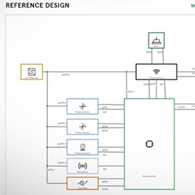
Avnet has made thousands of customizable reference designs easily accessible to engineers in the Americas in its new self-service online tool Design Hub.
Design Hub is powered by AVAIL, Avnet’s engineering tool with a vast reference design library that helps designers develop system-level solutions quickly and easily any time of day. The tool leverages more than 70,000 solutions to common design problems. These solutions are automatically loaded into the engineer’s design based on their specific requirements.
“Research shows that 80% of engineers use datasheets, application notes, reference designs and block diagrams to begin their new designs,” said Art Leitherer, vice president of Global Technology and Solutions for Avnet. “All of that research takes time, and if what they are looking for is new to them, asking the right questions to find the data can be challenging as well. Now they can leverage the Design Hub to take advantage of the community of designers that have assembled current and available content that is applicable to the need. Ultimately, it helps engineers create their designs faster by giving them visibility to products that are actually available and the knowledge to put them to use.”
Design Hub makes it easy for engineers to understand and access the information needed to get a project started. They can also customize and personalize information in a self-service tool that’s available 24/7. To help accelerate designs, engineers can make modifications and save work, determine if an idea or design can work within constraints, generate the documentation needed to jump start a project and feel comfortable knowing the information is secure through Avnet’s single sign on for customers.
Engineers will walk away with documentation including preliminary schematics and layouts as well as a bill of materials (BOM) for the design. It can even connect to CAD tools. This means the lifecycle status for all parts and overall BOM health will be available up front to ensure available parts are used in the design. Users can add parts to a quote or shopping cart or download the complete BOM with a single click.
“Our latest Avnet Insights research, out tomorrow, found engineers are leaning into their distributor relationships now more than ever. Design Hub allows us to add value to that distribution relationship,” explained Leitherer. “Before Design Hub, finding the right reference design was time consuming. Engineers had to search through a ton of supplier websites before finding what they needed. We bring all those reference designs to them in one place along with the tools to modify them to their needs. There are already over 1,000 free-to-use reference designs on the Avnet Americas Design Hub that cover state-of-the-art applications across the major categories and market verticals.”
Other Design Hub features also include software, calculators, simulators, cross-references, and other design and engineering tools that are typically associated with a key manufacturer’s products. These tools and resources can also be tied to a reference design that has simulation capabilities, or that requires a deeper level of engineering via software to arrive at the best possible solution.
Share on:


Suggested Items
Connect the Dots: Designing for Reality—The Pre-Manufacturing Process
05/08/2024 | Matt Stevenson -- Column: Connect the DotsI have been working with Nolan Johnson on a podcast series about designing PCBs for the reality of manufacturing. By sharing lessons learned over a long career in the PCB industry, we hope to shorten learning curves and help designers produce better boards with less hassle and rework. Episode 2 deals with the electronic pre-manufacturing process. Moving from CAD (computer-aided design) to CAM (computer-aided manufacturing) is a key step in PCB manufacturing. CAM turns digital designs into instructions that machines can use to actually build the PCB.
Indium Corporation to Showcase HIA Materials at ECTC
05/07/2024 | Indium CorporationAs an industry leader in innovative materials solutions for semiconductor packaging and assembly, Indium Corporation® will feature its advanced products designed to meet the evolving challenges of heterogeneous integration and assembly (HIA) and fine-pitch system-in-package (SiP) applications at the 74th Electronic Components and Technology Conference (ECTC), May 28‒31, in Denver, Colorado.
Siemens Delivers New Solido IP Validation Suite
05/07/2024 | SiemensSiemens Digital Industries Software introduced Solido™ IP Validation Suite software, a comprehensive, automated signoff solution for quality assurance across all design intellectual property (IP) types, including standard cells, memories and IP blocks.
Altair Acquires Research in Flight, Forging a New Path for Aerodynamic Analysis
05/07/2024 | AltairAltair a global leader in computational intelligence, announced it has acquired Research in Flight, maker of FlightStream®, which provides computational fluid dynamics (CFD) software with a large footprint in the aerospace and defense sector and a growing presence in marine, energy, turbomachinery, and automotive applications.
Happy’s Tech Talk #28: The Power Mesh Architecture for PCBs
05/07/2024 | Happy Holden -- Column: Happy’s Tech TalkA significant decrease in HDI substrate production cost can be achieved by reducing the number of substrate layers from conventional through-hole multilayers and microvia multilayers of eight, 10, 12 (and more), down to four. Besides reducing direct processing steps, yield will increase as defect producing operations are eliminated.